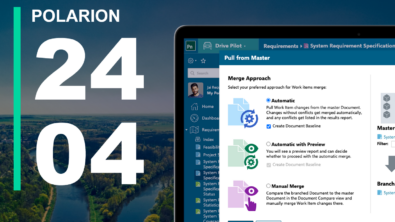
Archive for November, 2010
PCB Design Perfection Starts in the CAD Library – Part 7
Land Calculations
IPC-7351 for SMT technology defines the rules for creating optimized land pattern CAD library parts using a 3-Tier system – Least (high density), Nominal (controlled environment) and Most (ruggedized & shock resistant). Many PCB designers and CAD Librarians have heard about the IPC-7351B standard, but few people know how they work. The IPC LP Calculator has made life easy for the PCB design industry by automatically generating accurate land pattern data derived from component dimensions. Part 7 of this series will describe the basic fundamental aspects of defining the optimized land (pad) size for a CAD library part and the mathematical model of the LP Calculator.
Land (Pad) Size and Location:
These 7 factors are used to calculate the optimum Land Size –
-
Component Body Tolerance
-
Component Terminal Tolerance
-
Fabrication Tolerance
-
Placement Tolerance
-
Land Size Round-off
-
Land Spacing Round-off
-
Solder Joint Goals for Toe, Heel and Side

Component Lead Span

Component Terminal Tolerance
The Fabrication (Manufacturing) Tolerance compensates for the fabrication allowance for etch back. By adding a fabrication tolerance, we calculate the land area that we need after the fabrication etching process. If your manufacturer over-sizes the land areas during the CAM process to compensate for their own etching tolerances, this is referred to as “double tolerance” because of double compensation for the same allowance. Ask your manufacturer if they over-size the land features. If they do, tell them that you already compensated for that in your CAD library. The IPC-7351 fabrication tolerance is 0.05mm.

Fabrication Tolerance
The Placement (Assembly) Tolerance compensates for the pick and place machine accuracy. When parts are manually placed or machine placed, there is a small margin of placement accuracy that must be accounted for. The IPC-7351 assembly tolerance is 0.05mm.
Land Place (Spacing) Round-off relates to the land center to land center spacing. The goal in the IPC-7351 is to place all lands on a 0.05mm grid, so the space between the land span is rounded to 0.1mm increments so that the distance from the center of the land pattern to the center of the land is in 0.05mm increments. This plays a critical role in trace routing to achieve the highest packing density. In this picture example of a common Chip Component, the land snap grid is 0.05 mm from the center of the part to the center of the lands. The C1 & C2 dimensions.

Land Place and Size Round-off
Land Size Round-off is the value that the land size rounds up or down to. The IPC-7×51 standards round land sizes to 0.05mm increments with the exception of micro-miniature component packages that are typically less than 1.6mm in size. The micro-miniature part land size round-off is set to 0.01mm increments. In the picture above, the “X” & “Y” dimensions are rounded off in 0.05 mm increments. Even the land corner radius is rounded in 0.05 mm increments.
Solder Joint Goals for Toe are usually the outside the component lead with two exceptions, the J-Lead and the Molded Body components the Toe is under the component body. The Heel goals are normally on the inside of the component lead and the side goals are for both sides of the component lead. In Part 5 of this series I listed the component Lead Forms. Every lead form has it’s unique solder joint goal table. Here is a sample table for the Least, Nominal and Most “Toe, Heel and Side” goals and the Placement Courtyard Excess for the Gull Wing component family. Notice the Round-off factor is in 0.05 mm increments.

Gull Wing Solder Joint Goal Table
When all of the Tolerances, Round-offs and Solder Joint goals are applied the end result is a perfect land pattern.

Land Pattern & Component with Tolerances
If all the Tolerances and Solder Joint Goals were removed from the mathematical model, the component lead would be equal to the land size. This is the starting point for all land size calculations. The picture below illustrates a Chip Component (black) without Tolerances, Round-offs, or Solder Joint Goals and the land size (cyan).

Land Pattern & Component with no Tolerances
The resulting solder joint for a chip component should look similar to this picture. Note that the component terminal never touches the land. There must be solder paste between the component lead and the land to form the best solder joint. Here’s a note from the IPC J-STD-001D “Requirements for Soldered Electrical and Electronic Assemblies”. Section 4.14 Solder Connection: All solder connections shall indicate evidence of wetting and adherence where the solder blends to the solder surface.

Chip Solder Joint
Tags: CAD Libraries, Padstacks, PCB Design
PCB Design Perfection Starts in the CAD Library – Part 6
The IPC-7351B standard only focuses on 2 two major aspects of the CAD library:
- The land size and spacing
- Placement courtyard
All of the other aspects of the CAD library part such as silkscreen & assembly outlines, polarity markings, ref des, centroid marking, etc. are considered user definable drafting items. This includes all of the rules that pertain to these items such as line widths, silkscreen to land spacing, polarity sizes, ref des height, etc. are not part of the standard. But the Placement Courtyard Boundary is defined in the IPC-7351B standard, but the line width used to create the outline is user definable. The default solder mask and paste mask values are mentioned in the IPC-7351 as to be 1:1 scale of the land size, but this is only a recommendation.
See Courtyard Determination pictures below to see the 3 outlines defined by IPC-7351 as:
- Maximum Component Boundary
- Minimum Placement Courtyard
- Courtyard Manufacturing Zone

Surface Mount Courtyard Determination

Plated Through-hole Courtyard Determination
Here are the standard spacing rules from the Maximum Component Boundary to the Minimum Placement Courtyard:
- Least Environment = 0.1 mm
- Nominal Environment = 0.25 mm
- Most Environment = 0.5 mm
There are different Placement Courtyard spacing rules for Grid Array packages based on ball size:
- Ball size above 0.50 mm = 2 mm
- Ball size between 0.50 mm & 0.25 mm = 1 mm
- Ball size below 0.25 mm = 0.5 mm
One of the key aspects of the placement courtyard is that it allows room for rework. In the case of the BGA’s, the larger the Ball Size, the larger the heat nozzles and removal equipment is for getting around and under the component to unsolder the contacts. An important note to make here is that if you have no intentions of ever reworking (remove and replace) a BGA component then the 2 mm placement courtyard is not necessary and a 0.5 mm courtyard excess is OK. This also is relevant to the “Most Environment” where the minimum courtyard excess is 0.5 mm on all SMT land patterns. i.e.: the military and medical instrument industry might use the Most Environment and require “Class 3″ High Reliability Electronic Products where continued high performance is critical and product downtime cannot be tolerated. The “Class 3″ fabrication is very expensive and if a component on the PCB fails, rework becomes necessary to reduce cost. Rework requires additional land pattern placement courtyard excess to allow adequate space for rework equipment. Alternatively, the “Least Environment” for High Density PCB Layout, like handheld devices, has a courtyard excess of 0.1 mm with no room for rework equipment. So if a component fails in your Cellular Phone it will not be sent back to the shop for rework, but instead, it will be discarded.
The Placement Courtyards can be placed next to each other so the outline overlaps, however you need to discuss this with your assembly shop if they require an additional Manufacturing Zone for their process. The Placement Courtyard round-off snap grid is 0.5 mm. The question of “why don’t you place the silkscreen outline outside the land pattern boundary” is a FAQ and this is the answer - ”It is important that all silkscreen outline data be located inside the Placement Courtyard”.
This includes the Post Assembly Inspection Dot, which sometimes gets partially placed outside the placement courtyard. This is why in the upcoming IPC-2614 for Board Fabrication Documentation and drafting standards the “Post Assembly Inspection Dot” will become the “Post Assembly Inspection Line” and it will look like this to keep them inside the Placement Courtyard:

DIP & SOP Post Assembly Inspection Line

Axial Lead Courtyard
Most Enterprise CAD tools like Mentor Expedition have a different DRC checking feature that the user can define the component type to component type spacing rules. In this case, the placement courtyard excess should be turned off and the placement courtyard would be identical to the Maximum Component Boundary.

Enterprise CAD Tool Courtyard
The Enterprise CAD tool placement courtyard is not defined in the IPC-7351 standard. This concept is based on the Enterprise CAD tools ability to determine various component body to body spacing that is user definable.
Tags: CAD Library, PCB Design
About Tom Hausherr's Blog
New component package technology and CAD library standards.
Latest Posts
- PCB Design Perfection Starts in the CAD Library – Part 19
- PCB Design Perfection Starts in the CAD Library – Part 18
- PCB Design Perfection Starts in the CAD Library – Part 17
- PCB Design Perfection Starts in the CAD Library – Part 16
- PCB Design Perfection Starts in the CAD Library – Part 15 QFN
- Inch to Metric Conversion Tables for PCB design