Tecnomatix
Driving sustainable transformation: BSH's journey towards CO2 reduction in enamelling
April 25, 2024
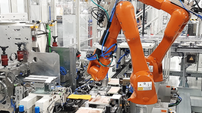
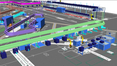
In today's global manufacturing landscape, the imperative for CO2 reduction shapes new paradigms in production planning. Mert Gök, an innovator at BSH Home Appliances Group, illuminates this journey in his presentation on sustainable transformation at the 2024 Plant Simulation User Conference. Delving into the critical enamelling process, essential in home appliance manufacturing, Gök explores strategies to minimize CO2 emissions. Through meticulous planning and execution, BSH achieves remarkable results, halving CO2 emissions while optimizing production efficiency. This holistic approach not only fosters environmental sustainability but also enhances operational excellence and corporate reputation. Join the discourse, as we navigate toward a greener, more sustainable future together.