Tecnomatix
User-friendly modeling and simulation of manual production lines
April 22, 2024
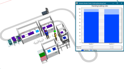
2024 Plant Simulation User Conference presentation by Robert Bosch and Siemens Industry Software on user-friendly modeling and simulation for manual production lines. At Robert Bosch GmbH's Working Group Digital Production, Tobias Lechler, Melanie Wolf, and their team are focusing on improving manual production line planning and execution. Through user-friendly modeling and simulation techniques, they've developed a standard library that streamlines the modeling process, offering benefits such as reduced effort and automated model generation. Their approach holds promise for enhancing manufacturing efficiency and productivity.